1. What is a Microstrip Mitred Bend Calculator?
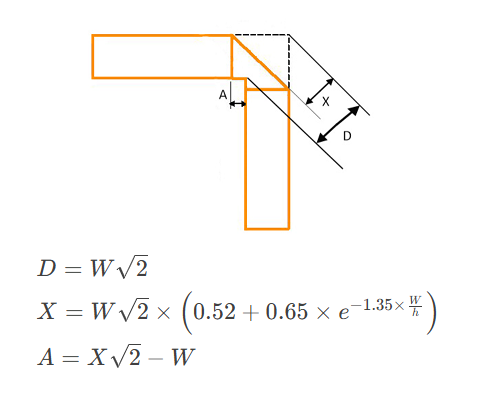
Definition: This calculator determines the dimensions of a mitred bend in a microstrip transmission line, specifically the diagonal length (\( D \)), offset distance (\( X \)), and mitred cut length (\( A \)), based on the microstrip width (\( W \)) and substrate height (\( h \)).
Purpose: It helps RF and PCB designers optimize 90-degree bends in microstrip lines to minimize signal reflections and maintain impedance, crucial for high-frequency circuit performance.
2. How Does the Calculator Work?
The calculator uses the following formulas to compute the mitred bend dimensions:
Diagonal Length \( D \):
\[
D = W \sqrt{2}
\]
Offset Distance \( X \):
\[
X = W \sqrt{2} \times \left(0.52 + 0.65 \times e^{-1.35 \times \frac{W}{h}}\right)
\]
Mitred Cut Length \( A \):
\[
A = X \sqrt{2} - W
\]
Where:
- \( D \): Diagonal length of the mitred bend
- \( X \): Offset distance for the mitred cut
- \( A \): Length of the mitred cut
- \( W \): Width of the microstrip line
- \( h \): Substrate height (distance to ground plane)
Unit Conversions:
- Input Dimensions (\( W, h \)):
- 1 mm = 39.3701 mils
- 1 μm = 0.0393701 mils
- Output Dimensions (\( D, X, A \)):
- 1 mil = 0.0254 mm
- 1 mil = 25.4 μm
Steps:
- Enter the microstrip width \( W \) and substrate height \( h \), selecting the unit for each (mils, mm, or μm).
- Click "Calculate" to compute \( D \), \( X \), and \( A \).
- The results are initially displayed in mils.
- Select a different unit for each dimension (mils, mm, or μm) from the dropdowns after each result to convert the displayed values.
3. Importance of Microstrip Mitred Bend Calculation
Calculating the dimensions of a mitred bend is essential for:
- Signal Integrity: Minimizes reflections at 90-degree bends, preserving signal quality in high-frequency circuits.
- Compact Design: Allows for efficient PCB layouts by enabling sharp turns without significant performance loss.
- Impedance Control: Helps maintain the characteristic impedance of the microstrip line around bends.
4. Using the Calculator
Examples:
- Example 1: \( W = 19.685 \) mils, \( h = 25 \) mils, Results in mils
- \( D = 19.685 \times \sqrt{2} \approx 27.83 \, \text{mils} \)
- \( X = 19.685 \times \sqrt{2} \times \left(0.52 + 0.65 \times e^{-1.35 \times \frac{19.685}{25}}\right) \approx 23.96 \, \text{mils} \)
- \( A = 23.96 \times \sqrt{2} - 19.685 \approx 14.21 \, \text{mils} \)
- Example 2: \( W = 0.5 \) mm, \( h = 635 \) μm, Results in μm
- Convert: \( W = 0.5 \times 39.3701 \approx 19.685 \, \text{mils} \), \( h = 635 \times 0.0393701 \approx 25 \, \text{mils} \)
- Same as Example 1: \( D \approx 27.83 \, \text{mils} \), \( X \approx 23.96 \, \text{mils} \), \( A \approx 14.21 \, \text{mils} \)
- Results in μm: \( D = 27.83 \times 25.4 \approx 706.88 \, \text{μm} \), \( X = 23.96 \times 25.4 \approx 608.58 \, \text{μm} \), \( A = 14.21 \times 25.4 \approx 360.93 \, \text{μm} \)
- Example 3: \( W = 19.685 \) mils, \( h = 0.635 \) mm, \( D \) in mm, \( X \) in μm, \( A \) in mils
- Convert: \( h = 0.635 \times 39.3701 \approx 25 \, \text{mils} \)
- Same as Example 1: \( D \approx 27.83 \, \text{mils} \), \( X \approx 23.96 \, \text{mils} \), \( A \approx 14.21 \, \text{mils} \)
- Results: \( D = 27.83 \div 39.3701 \approx 0.71 \, \text{mm} \), \( X = 23.96 \times 25.4 \approx 608.58 \, \text{μm} \), \( A \approx 14.21 \, \text{mils} \)
5. Frequently Asked Questions (FAQ)
Q: What is a microstrip mitred bend?
A: A microstrip mitred bend is a 90-degree turn in a microstrip transmission line where the corner is chamfered (mitred) to reduce signal reflections and maintain impedance, improving performance in RF circuits.
Q: Why are mitred bends used in microstrip lines?
A: Mitred bends minimize reflections and capacitance at sharp corners, preserving signal integrity in high-frequency applications where space efficiency is critical.
Q: What factors affect the accuracy of these calculations?
A: The formulas assume ideal conditions. Real-world factors like frequency-dependent effects, dielectric variations, and manufacturing tolerances can affect accuracy. For precise designs, simulations may be required.
Microstrip Mitred Bend Calculator© - All Rights Reserved 2025
 Home
Home
 Back
Back